|
Microwaves & RF
August 1999

Synthesis + Simulation = Enhanced Design Process
The combination of circuit
synthesis and simulation functions within a common CAE design tool can
greatly improve the RF/microwave-design process.
By Dale D. Henkes
President
Applied
Computational Sciences, 1061 Dragt Pl., Escondido, CA 92029; (760) 612-6988
e-mail: LINC2@appliedmicrowave.com,
Internet: www.appliedmicrowave.com
CIRCUITS can be created in several different ways with
computer-aided-engineering (CAE) techniques. With a circuit-synthesis
program, a designer starts by entering a list of specifications or design
goals and pushing the "synthesize" button. Another approach might
be to borrow a circuit topology from an existing design and then start a
simulation program optimizing the circuit against a set of design goals.
Perhaps the best approach, however, is to combine synthesis and simulation
within the same CAE tool.
The synthesis approach to circuit design is more direct, but it may or may
not provide the user enough flexibility in influencing the outcome. However,
a well-designed synthesis program will attempt to provide the user with as
much control over the final design as possible (or practical). This may
include accepting a wide variety of input from the user, a choice of circuit
topology, or both. After the design has been synthesized, it can then be
analyzed in a circuit-simulation program to verify performance according to
the engineer's requirements. Optimization or tuning can be used at this stage
to tweak the design. Therefore, a complete set of design tools would include
synthesis and simulation.
The design-by-simulation/optimization method is often a trial-and-error
approach with no guarantee of success. An impedance-matching problem, for
example, may not be solvable with the circuit topology presented to the
optimizer. Worse than that is the fact that, because it cannot change the
circuit topology (only the component values), the optimizer might get close
to meeting an impossible goal by adjusting some circuit component's value to
a very large or extremely small value that would not be practical or
obtainable.
The MicroLINC™ program from Applied Computational Sciences (Escondido, CA)
combines RF and microwave-circuit analysis (simulation) with a set of synthesis
tools. One of the most comprehensive circuit-synthesis tools in the package
is the "Circles Utility." Primarily a small-signal amplifier or
low-noise-amplifier (LNA) design tool, this module is aimed at synthesizing
input and output matching networks for the active device. The active device
is usually a transistor [bipolar or field-effect-transistor (FET)] that is
characterized by a set of S-parameters.
The philosophy behind this utility is to give the user as much or as
little input into the synthesis processes as desired. In keeping with that
philosophy, a substantial amount of analyses and data are available to assist
the designer (Fig. 1).
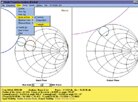
Fig 1. The MicroLINC CAE program combines synthesis and simulation,
providing users with a great deal of analysis power through pull-down menus.
Thus, a designer experienced in the use of noise, gain, and stability
circles can take advantage of the highly automated, yet interactive, nature
of these tools as a guide to developing the best design that meets the requirements.
On the other hand, a novice might simply input a gain specification and then
select a default-matching network from the "Match" menu. The result
is the creation of the entire circuit, seamlessly integrated into the
simulator for immediate analysis and performance verification. All that
remains to be done is to push the "Analyze Circuit" button for
generating simulation results.
This is not to imply that a novice designer could not benefit from the
circle utilities. Indeed, the interactive nature of the tool encourages
experimentation. For example, a tool that proves as useful to the novice as
it is to an experienced designer is the "Noise and Gain Trade-offs"
tool shown in Fig. 1. When this is selected, gain and noise circles appear on
the Smith Chart in the input plane. The circles automatically intersect at a
common impedance point representing a typical compromise between maximum gain
and minimum noise figure. A slider control below the Smith Chart points
toward "Max Gain" on the left or "Min Noise" on the
right.
Gain and noise-figure (NF) trade-offs can be viewed instantly by sliding
the control toward Max Gain or Min Noise. As this is performed the gain and
noise circles stay locked together, intersecting at the source reflection coefficient
( s)
as it moves along an optimum path between minimum noise and maximum gain. The
gain and noise data are updated at the bottom of the screen so the user can
determine when the appropriate trade-off has been made. As soon as a suitable
trade-off between noise and gain is found, the program has all the data it
needs to design the circuit. The next step is to select a set of matching
networks from a list of various lumped and distributed topologies. Clicking
on one of the items in the list automatically completes the circuit and
generates the component values. It is possible to learn an effective design
methodology simply by using this feature of MicroLINC. s)
as it moves along an optimum path between minimum noise and maximum gain. The
gain and noise data are updated at the bottom of the screen so the user can
determine when the appropriate trade-off has been made. As soon as a suitable
trade-off between noise and gain is found, the program has all the data it
needs to design the circuit. The next step is to select a set of matching
networks from a list of various lumped and distributed topologies. Clicking
on one of the items in the list automatically completes the circuit and
generates the component values. It is possible to learn an effective design
methodology simply by using this feature of MicroLINC.
DESIGN EXAMPLE
To further illustrate the design process using CAE techniques, the
following design example is proposed:
1. The task involves the design of an amplifier with 12-dB gain at 6.365
GHz using an NEC NE76038 low-noise GaAs metal-semiconductor FET (MESFET) from
NEC/California Eastern Laboratories (Santa Clara, CA) biased at a
drain-source voltage of VDS = +3 VDC and a drain-source current of
IDS = 10 mA.
2. The transistor must be stabilized within the operating band with both
ports simultaneously matched [designed for maximum available gain (MAG) after
stabilization].
3. The input port must be matched to an impedance of 75 while
the output port is matched to 50. while
the output port is matched to 50.
4. The amplifier's NF must then be determined when the amplifier has been
matched for maximum gain.
5. The amplifier circuit should be synthesized using distributed
(transmission-line) matching networks.
6. Simulation should be used to verify the gain and impedance-matching
conditions.
Determine the amplifier's NF when matched for maximum gain.
With the MicroLINC Circles Utility, these six apparently complex steps
take only a few minutes to accomplish. First, the NE76038 transistor's
S-parameter file is opened and 6365 MHz is selected from the
"Frequency" menu. Selecting "Maximum Gain...MAG" from the
view menu reveals that it is unavailable. Attempting to match both ports to
obtain the MAG fails because the device by itself is potentially unstable at
this frequency. This is quickly verified by selecting "View
Stability" and noting that the stability circles cut into the upper left
part of the Smith Chart. Additionally, the stability factor reported is less
than 1 (k = 0.799).
The Circles Utility provides several ways to stabilize a potentially
unstable device. The method used here will be to place a small amount of
inductance in the common (source) lead of the transistor. (Reference 1 points
out some of the advantages of using this method). Selecting "Common Lead
Inductance" from the "Stabilize Device" menu (Fig. 2)
and clicking the "Optimize" button automatically inserts the
minimum amount of inductance needed to stabilize the device at the design
frequency. If "Include Noise" is checked, then the noise parameters
of the device will be adjusted to include the effects of the inductor.
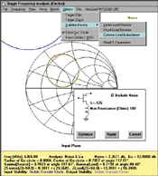
Fig 2. Stabilizing a high-frequency transistor for use in a microwave
amplifier is a simple matter when using the "Stabilize Device" menu
selection.
The next step is to change the input impedance from the 50-
default to 75 via
the "Options... Target Z0in" menu. Selecting
"Maximum Gain... MAG" from the view menu now displays the optimum
match points for maximum gain (~12.09 dB). The result is a single point
(impedance match) in each of the input and output planes. This is referred to
as a bilateral simultaneous conjugate match.2 It is
considered a bilateral match because the program solves the matching problem
at both ports simultaneously, taking into account the fact that S12
is a nonzero value (the output match affects the input match and vice versa).
The selection "View...Noise and Ga" displays the noise circle that
intersects the MAG point in the input plane. The NF is reported as ~2.27 dB
at a gain of 12.09 dB as shown in Fig. 2. The program now has all the
information it needs to complete the circuit. Selecting "Transmission
Line...Stub and TRL Cascade" from the "Match" menu produces
the circuit shown in Fig. 3.
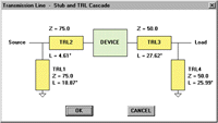
Fig 3. This circuit contains the matching input and output networks
needed to meet the 75- and 50- input
and output conditions, respectively.
Then, the circuit file is automatically constructed and placed in the Text
Editor (Fig. 4) for viewing and subsequent analysis.
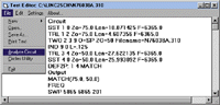
Fig 4. This circuit file represents the schematic diagram of Fig. 3. It
is automatically generated and placed in MicroLINC's Text Editor for viewing
and analysis.
SIMPLE SIMULATION
"Analyze Circuit" starts the simulation, producing the results
shown in Figs. 5 and 6.
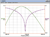
Fig 5. The simulated performance of the example amplifier is shown here
for gain (M21) and return-loss (M11) characteristics
centered at the design frequency.
Figure 5 indicates that the gain specification has been met, while Fig.
6 shows the quality of the input and output match.
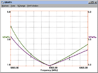
Click
to see enlarged image
Fig 6. The plot above shows the quality of the input as well as output
impedance-matching networks for the example amplifier.
The marker at 6365 MHz indicates that the input has been matched to 75 with a
VSWR of 1.01:1 and the output is matched to 50 with
approximately the same VSWR. An excellent match at both ports was expected
(and obtained) because that is what was requested of the synthesizer when it
was invoked to perform a MAG design.
Figure 7 shows that the additional goal of in-band transistor
stabilization has been met.
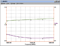
Click
to see enlarged image
Fig 7. This plot illustrates the effectiveness of matching the
transistor for high gain while maintaining good in-band operating stability.
As indicated, the Rollett Stability factor (k) is greater than 1 while the
absolute value of the determinant of the S-parameter matrix, | |, is
substantially less than 1 over the 1-GHz band around the operating frequency.
This ensures that the transistor is unconditionally stable at the operating
frequency. Of course, additional steps will need to be taken to ensure that
the amplifier will be stable at all frequencies. Components can be built into
the DC bias feeds in such a way as to enhance stability above and below the
operating frequency. |, is
substantially less than 1 over the 1-GHz band around the operating frequency.
This ensures that the transistor is unconditionally stable at the operating
frequency. Of course, additional steps will need to be taken to ensure that
the amplifier will be stable at all frequencies. Components can be built into
the DC bias feeds in such a way as to enhance stability above and below the
operating frequency.
This completes the initial RF portion of the design. The MicroLINC
"Transmission Lines" tool can be used to generate the physical
dimensions for printed-circuit-board (PCB) microstrip or stripline designs
from the electrical parameters shown in Fig. 3.
In closing, it should be noted that simulation provides much more than
just verification of the synthesized design. Simulation provides more
performance analysis (and insight into circuit behavior) than could be known
at the time of circuit synthesis. For example, the return loss (M11)
in Fig. 5 gives an indication of the narrowband nature of the input match.
Additionally, Monte Carlo analysis (from the MicroLINC statistics module) can
indicate the amplifier's sensitivity to component tolerances. However, design
by simulation alone is a trial-and-error approach. Therefore, when selecting
an RF CAE program, it is a good idea to consider a package that provides
synthesis and analysis capabilities.
In comparison, a design engineer can spend a great deal of time (and cost)
on a combination of separate programs, such as impedance-matching tools,
linear circuit simulators, and synthesis software, hoping that the tools mesh
and can seamlessly share files. A more practical approach is to select a
single tool with multiple functions, so that design files are not lost or
outdated when an independent software tool is upgraded.
References
1. Dale D. Henkes, "LNA Design Uses Series Feedback to Achieve
Simultaneous Low Input VSWR and Low Noise," Applied Microwave &
Wireless, October 1998, p. 26.
2. Guillermo Gonzalez, Chap. 3, Sec. 3.6, "Simultaneous Conjugate
Match--Bilateral Case," in Microwave Transistor Amplifiers,
Prentice-Hall, Englewood Cliffs, NJ, 1984.
|