|
August
2002
RF Design Tool Matches Two Ports
Simultaneously
for Both Active and Passive Devices
by Dale Henkes, Applied Computational Sciences
For many
RF and microwave circuits it is important to efficiently transfer the
maximum possible amount of power available from a given power source to a
load. Often it is necessary to amplify or modify the signal power in some
way before it is delivered to the load.
When the signal power travels through a modifying device or sub-circuit,
there are two interfaces involved in the power transfer. At each
interface where power flows into or out of the circuit (input and output
ports) the impedance on one side of the interface must be numerically
equal to the complex conjugate of the impedance on the other side or
maximum power transfer will not occur as desired. At each interface where
the complex conjugate “match” does not exist, an impedance “matching
network” must be provided to transform the impedances into the conjugate
matched state.
Many circuit simulation programs are available that can analyze a circuit
to determine how well it is matched to a given source or load impedance.
Computer programs that can only do simulation are sometimes used to
design the matching circuits by an iterative process of tuning and
optimization. One problem with this approach is that the circuit topology
has to be known before it can be presented to the simulator for analysis
and subsequent optimization of the component values. Additional problems
arise when the designer selects a circuit topology that is incapable of
providing the required impedance transformation. The result is a lot of
wasted time running an optimization process that never converges to the
desired goal.
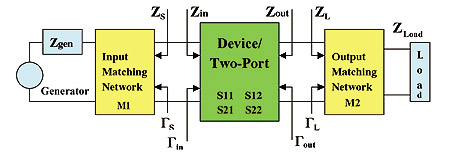
Figure 1: Two-port Impedance Matching
Fewer
programs actually provide tools to design the matching networks. Some
provide utilities to facilitate the design of a matching network for a
single port. But, fewer still provide utilities for designing networks
for matching two ports simultaneously. (It will be shown below why this
distinction is important). This article describes how the LINC2 design
and simulation program from ACS automates the process of designing
networks to match both input and output ports simultaneously.
The general problem of impedance matching a device (represented by its
two-port S Parameters) to a given source and load termination is shown in
Figure 1. The solution, resulting in the overall circuit producing
maximum available gain, is an input matching network, M1, and an output
matching network, M2, which will provide conjugate matching at both ports
simultaneously. However, it should be noted that a conjugate match at
both ports can only be achieved if the device is unconditionally stable.
In the example in this article, a device will be used that meets this
stability criterion.
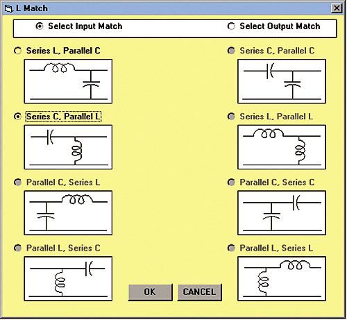
Figure 3: The L-Match Menu
The LINC2
program provides a utility that can be used to automatically solve the
matching problem for the general case, where the device is bilateral. In
this case S12=0 and Zin and Zout are NOT simply equal to S11 and S22
respectively:
 in =
S11 + S12 S21 L/(1
- S22 L) in =
S11 + S12 S21 L/(1
- S22 L)
Equation 1
out
= S22 + S12 S21 S/(1
- S11 S)
Equation 2
Zin = Z0
(1 + in)/(1
- in)
Equation 3
Zout = Z0
(1 + out)/(1
- out)
Equation 4
The goal
is to make ZS = Zin* and ZL = Zout*. The determination of Zin and Zout is
required before the matching networks can be designed, but calculation of
Zin and Zout is not easy to do manually. The reason is that Zin depends
on ZL. But ZL depends on Zout which in turn is a function of ZS which
depends on Zin. This is completely circular since we were trying to find
Zin in the first place. A similar situation exists when trying to
determine the value of Zout. This problem can only be solved by writing
two complex simultaneous equations in the variables Zin and Zout.
Calculation of Zin and Zout to obtain ZS and ZL is most efficiently done
by using a computer program such as LINC2. LINC2 not only finds the ZS
and ZL that yield a simultaneous conjugate match but automatically
designs the matching networks as well.
Use of the LINC2 tool to design matching networks for an active device
was presented in an article in the December 2001 issue of MPD (see “RF
Design Software Combines Synthesis and Simulation” on page 12 of the
December 2001 issue of MPD). The example in this article will focus on
using this tool to design the matching networks for a passive device. The
two-port passive device requiring matching to 50 ohms is an IF monolithic
crystal filter for 183.6 MHz.
|
|
|
|
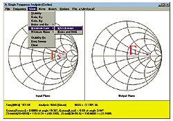
Figure 2: Device
Terminations for
Simultaneous Matching
Click to enlarge
|
Figure 7:
Simulated S21
Click to enlarge
|
|
|
|
|
Figure 6:
Simulated S11 and S22
Click to enlarge
|
Figure 8:
Measured Zin and Zout
Click to enlarge
|
Design
Example– matching a monolithic crystal filter to 50 ohms
The filter in this example was intended for use as an IF filter in an
AMPS cellular telephone with an IF frequency of 183.6 MHz. The
manufacturer specifies that the insertion loss of the filter will be less
than 4.5 dB and that the -3 dB passband edges will be at least +/-13 KHz
from the passband center. Additionally, the match at both ports should
provide a return loss better than 10 dB (about 2:1 VSWR) over the band
defined by 183.6 MHz +/- 11 KHz. There are other specifications, such as
stop band attenuation, but we will focus on these three here because
these are the ones that we can influence most with our matching networks.
Our design goal then becomes:
Filter’s
nominal passband center: fn = 183.6 MHz
Insertion loss (IL): 4.5 dB max.
Maximum Passband Attenuation (fn +/- 13 KHz): IL + 3 dB
Match input port to 50 ohms: >10 dB return loss (from 183.589 MHz to
183.611 MHz)
Match output port to 50 ohms: >10 dB return loss (from 183.589 MHz to
183.611 MHz)
The
Design Procedure
The design procedure consists of measurement of the device’s S
Parameters, synthesis of the matching circuits, simulation of the circuit
design, building the prototype, and finally verification through
measurement that the hardware meets the design goals. The following steps
outline this process:
1. Measure
the Device’s S Parameters
Measure the S Parameters of the filter mounted alone on the circuit board
without matching networks. (When the S Parameters are available from the
device manufacturer this step is unnecessary). Store these “Device” S
Parameters on a data disk and transfer to a computer running the LINC2
design and simulation program.
2.
Determine the Required S
andL
from the Device’s S Parameters
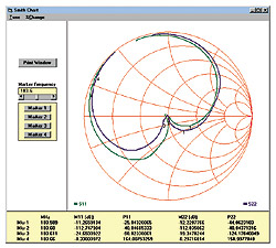
Load the device’s S Parameter file into the LINC2 Circles Utility and
select “Maximum Gain” from the “View” options. After selecting 183.6 MHz
from the frequency menu, the conjugate match points (S
and L)
will be displayed in the input and output planes respectively as shown in
Figure 2. These are the source and load reflection coefficients
that will properly match the filter. Their numeric values are printed at
the bottom of the screen along with their equivalent impedance values
(Zsource and Zload). Although this information is interesting (and even
necessary for anyone attempting to design the matching circuits manually)
the program does not require the user to do anything with S, L,
Zsource or Zload. That is because LINC2 synthesizes the matching circuits
automatically (next step in the design procedure).
3.
Synthesize the Matching Networks
As shown in Figure 2, the program calculated the optimum source
and load terminations required to properly match the device and yield the
Maximum Available Gain (MAG). The LINC2 Circles Utility reports that the
MAG in this case is -3.14 dB. This suggests that more than 1 dB of margin
can be achieved over the insertion loss spec (4.5 dB max). Matching to 50
ohms is assumed by default but this can be changed (from the Options
menu) for either or both port 1 and port 2. The next step is to select
the desired type of matching networks from a list of available circuit
topologies displayed in the “Match” menu. The networks available include
“L”, “PI”, “T”, and networks consisting of various distributed
(transmission line) elements. In this example the “L” match was chosen as
shown in Figure 3.
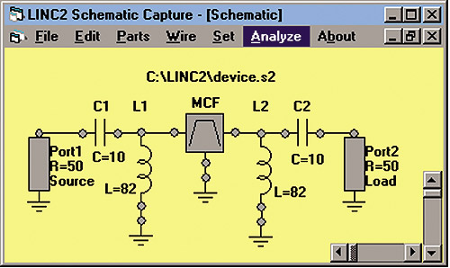
Figure 5: The Circuit Schematic
A palette
of all 8 possible “L” configurations are displayed. In this case only two
of the 8 “L” networks are capable of solving the given matching problem.
The user is guided to the correct choices by making only the valid ones
selectable. The two valid choices consist of one low pass and one high
pass structure. In this example the high pass structure was selected for
both ports. This places an inductor in shunt across the port terminals of
the device and has the advantage of utilizing the series capacitor as a
DC block as well as a matching component. Clicking “OK” accepts this
choice and automatically generates the netlist of the complete filter
circuit, including the device and both input and output matching networks
as shown in Figure 4. The equivalent LINC2 schematic is shown in Figure
5 with component values rounded to their nearest standard values.
 4. Simulate the
Completed Circuit 4. Simulate the
Completed Circuit
At this point the circuit configuration and all component values have
been generated automatically by the LINC2 program. Simulation results can
be viewed immediately by selecting “Analyze” from the menu bar in the
netlist window (Figure 4- Text Editor). Alternatively, a circuit
schematic can be created in the schematic window and the simulation
launched from there (Figure 5). In either case the simulation
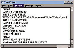
begins by selecting “Analyze” from the menu bar.
Figure
4: The Circuit Netlist
5.
Compare Simulation Results to Design Goals
LINC2 facilitates the characterization of circuit performance by offering
a variety of methods for displaying simulation data. Data can be
displayed in tabulated numerical form or by various graphical methods,
including the Smith Chart and Graph windows shown in Figures 6 and 7.
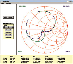
In Figure 6 the dB magnitude of S11 is displayed under the heading
M11 and its phase under the heading P11. S22 is similarly displayed. Figure
7 is a plot of the dB magnitude of S21 (labeled M21).
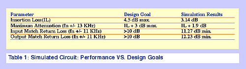
Table 1 summarizes the
simulated circuit’s performance and compares it to the design goals.
Since all of the design goals listed in Table 1 have been met, the
design can proceed to the next step, which is to build the prototype.
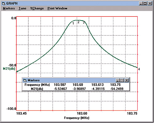
Figure 9: Measured S21
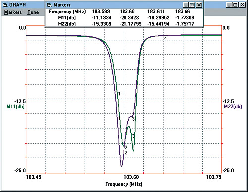
Figure 10: Measured S11 and S22
6.
Build and Test the Physical Prototype Circuit
The physical circuit was constructed on a printed circuit board using the
components shown in the schematic diagram (Figure 5). The
frequency response and the performance of the port matching were measured
with an Agilent 8753ES Vector Network Analyzer (VNA). This data was
captured from the VNA in an S Parameter file and imported into the LINC2
program for display. The measured data from the 8753ES VNA is displayed
in Figures 8, 9 and 10. As indicated in Figure 8, the resistive
part of the match at the input and output ports is approximately equal to
48 and 45 ohms respectively with less than 10 ohms of reactance. This
results in a return loss of better than 20 dB for both ports at the
design frequency of 183.6 MHz (see Figure 10). The minimum return loss
over the matching bandwidth (183.589 - 183.611 MHz) is about 11.2 dB as
shown in Figure 10. Figure 9 indicates that the insertion
loss is less than 4 dB at the nominal center frequency. The maximum
attenuation in the passband occurs at 183.587 MHz and is 1.57 dB greater
than the insertion loss (difference in S21 between markers 1 and 2 in Figure
9). All of the measured data came in better than the design goal,
even though the circuit was constructed with parts having component
values equal to the nearest standard values relative to the computer
synthesized values and the circuit was not “tuned”.
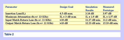
Table 2 summarizes the measured performance of the prototype circuit
and compares it to the design goal and simulation results. The prototype
circuit met all the design goals on the first cut without tuning. Also,
the simulation did an excellent job of predicting the performance of the
physical prototype filter circuit.
Although
tuning of the matching networks was not required in order to meet the
design parameter goals, two small adjustments in component values
resulted in a near perfect match at both ports of the prototype circuit.
The computer generated circuit called for a 92 nH shunt inductor at the
output side of the filter. The nearest standard value of 82 nH was used
for this inductor in constructing the physical circuit. Placing a 0.5 pF
capacitor in parallel with the 82 nH inductor brought the combined
reactance closer to the value calculated by the LINC2 program. Also, the
value of the series input capacitor was increased by 10%. With these two
changes to the initial prototype circuit, the input and output port
impedances improved to Zinput = 49 + J 0.2 and Zoutput = 52 - J 4 ohms
respectively. This resulted in measured return losses of better than 36
and 26 dB respectively for the two ports.
“Integrated design environment” are the buzzwords used in the Electronic
Design Automation (EDA) software industry today to describe the ability
of the software to solve a complex problem or complete a project through
the efficient linking of different but related tasks. Beyond the
integration of design tools and tasks, the program’s usefulness is
enhanced by its ability to interface with the outside environment. LINC2
can export circuit netlist files that can be read by other programs and,
more fundamentally, import and export data in industry standard S
Parameter files. This allows a convenient interface to RF test equipment
in the lab. The usefulness of having an industry standard data interface
was demonstrated at both the front end and the back end of this example
project. At the start of the project the device data was extracted using
a vector network analyzer and imported directly into the program’s
matching network synthesis tool. After the prototype circuit was
constructed and tested the measured data was returned to the LINC2
program for design verification and documentation. Documenting the
prototype’s performance could consist of replicating the instrument’s
displays in LINC2 for inclusion into a word processor document (as was
done in writing this article). Also, the data can be archived and later
recalled by the program for further analysis such as displaying the
filter’s group delay or changing the frequency of the marker data
readouts.
As shown here, a project can flow smoothly from design to verification
using LINC2 because the program couples schematic capture and a suite of
RF design tools to a powerful simulator engine. The entire design in this
example was completed in a matter of minutes. More information on LINC2
can be found on the Web at www.appliedmicrowave.com.
APPLIED COMPUTATIONAL
SCIENCES
Enter Reader Service No. 91
|